 | –≠–ª–µ–∫—Ç—Ä–æ–Ω–Ω—ã–π –∫–æ–º–ø–æ–Ω–µ–Ω—Ç: TCMD4000 | –°–∫–∞—á–∞—Ç—å:  PDF PDF  ZIP ZIP |
TCMD1000 / TCMD4000
Document Number 83513
Rev. 1.6, 26-Oct-04
Vishay Semiconductors
www.vishay.com
1
17298
C
C
E
A
C
4 PIN
16 PIN
1
2
8
9
Pb
Pb-free
e3
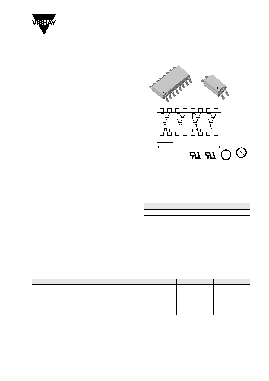
Optocoupler, Photodarlington Output, High Gain, Single/Quad
Channel, Half Pitch Mini-Flat Package
Features
∑ Low profile package (half pitch)
∑ AC Isolation test voltage 3750 V
RMS
∑ Low coupling capacitance of typical 0.3 pF
∑ Low temperature coefficient of CTR
∑ Wide ambient temperature range
∑ Lead-free component
∑ Component in accordance to RoHS 2002/95/EC
and WEEE 2002/96/EC
Agency Approvals
∑ UL1577, File No. E76222 System Code M, Double
Protection
∑ CSA 22.2 bulletin 5A, Double Protection
Applications
Programmable logic
Modems
Answering machines
General applications
Description
The TCMD1000 / TCMD4000 consist of a photodar-
lington optically coupled to a gallium arsenide infra-
red-emitting diodes in either a 4 pin or 16 pin miniflat
package.
The elements provide a fixed distance between input
and output for highest safety requirements.
Order Information
Absolute Maximum Ratings
T
amb
= 25 ∞C, unless otherwise specified
Stresses in excess of the absolute Maximum Ratings can cause permanent damage to the device. Functional operation of the device is
not implied at these or any other conditions in excess of those given in the operational sections of this document. Exposure to absolute
Maximum Rating for extended periods of the time can adversely affect reliability.
Input
Part
Remarks
TCMD1000
CTR > 600 %, SMD-4
TCMD4000
CTR > 600 %, SMD-16
Parameter
Test condition
Symbol
Value
Unit
Reverse voltage
V
R
6
V
Forward current
I
F
60
mA
Forward surge current
t
p
10 µs
I
FSM
1.5
A
Power dissipation
P
diss
100
mW
Junction temperature
T
j
125
∞C
www.vishay.com
2
Document Number 83513
Rev. 1.6, 26-Oct-04
TCMD1000 / TCMD4000
Vishay Semiconductors
Output
Coupler
1)
Related to standard climate 23/50 DIN 50014
Electrical Characteristics
T
amb
= 25 ∞C, unless otherwise specified
Minimum and maximum values are testing requirements. Typical values are characteristics of the device and are the result of engineering
evaluation. Typical values are for information only and are not part of the testing requirements.
Input
Output
Coupler
Parameter
Test condition
Symbol
Value
Unit
Collector emitter voltage
V
CEO
35
V
Emitter collector voltage
V
ECO
7
V
Collector current
I
C
80
mA
Collector peak current
t
p
/T = 0.5, t
p
10 ms
I
CM
100
mA
Power dissipation
P
diss
150
mW
Junction temperature
T
j
125
∞C
Parameter
Test condition
Symbol
Value
Unit
AC isolation test voltage (RMS)
V
ISO
1)
3750
V
RMS
Total power dissipation
P
tot
250
mW
Operating ambient temperature
range
T
amb
- 40 to + 100
∞C
Storage temperature range
T
stg
- 40 to + 100
∞C
Soldering temperature
T
sld
240
∞C
Parameter
Test condition
Symbol
Min
Typ.
Max
Unit
Forward voltage
I
F
= 50 mA
V
F
1.25
1.6
V
Junction capacitance
V
R
= 0 V, f = 1 MHz
C
j
50
pF
Parameter
Test condition
Symbol
Min
Typ.
Max
Unit
Collector emitter voltage
I
C
= 100
µA
V
CEO
35
V
Emitter collector voltage
I
E
= 100
µA
V
ECO
7
V
Collector dark current
V
CE
= 10 V, I
F
= 0, E = 0
I
CEO
100
nA
Parameter
Test condition
Symbol
Min
Typ.
Max
Unit
Collector emitter saturation
voltage
I
F
= 10 mA, I
C
= 1 mA
V
CEsat
0.3
V
Cut-off frequency
I
F
= 10 mA, V
CE
= 5 V,
R
L
= 100
f
c
10
kHz
Coupling capacitance
f = 1 MHz
C
k
0.3
pF
TCMD1000 / TCMD4000
Document Number 83513
Rev. 1.6, 26-Oct-04
Vishay Semiconductors
www.vishay.com
3
Current Transfer Ratio
Switching Characteristics
Typical Characteristics (Tamb = 25
∞C unless otherwise specified)
Parameter
Test condition
Part
Symbol
Min
Typ.
Max
Unit
I
C
/I
F
V
CE
= 2 V, I
F
= 1 mA
TCMD1000
CTR
600
800
%
TCMD4000
CTR
600
800
%
Parameter
Test condition
Symbol
Min
Typ.
Max
Unit
Rise time
V
CE
= 2 V, I
C
=10 mA,
R
L
= 100
(see figure 1)
t
r
300
µs
Turn-off time
V
CE
= 2 V, I
C
=10 mA,
R
L
= 100
(see figure 1)
t
off
250
µs
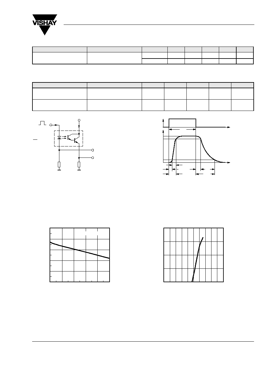
Figure 1. Test circuit, non-saturated operation
R
L
50
Channel II
Channel I
I
C
= 10 mA;
+V
CC
I
F
I
F
0
R
G
= 50
t
p
t
p
= 50
ms
T
= 0.01
Oscilloscope
R
I
= 1 M
C
I
= 20 pF
14779
Figure 2. Switching Times
t
p
t
t
0
0
10%
90%
100%
t
r
t
d
t
on
t
s
t
f
t
off
I
F
I
C
96 11698
t
p
pulse duration
t
d
delay time
t
r
rise time
t
on
(= t
d
+ t
r
)
turn-on time
t
s
storage time
t
f
fall time
t
off
(= t
s
+ t
f
)
turn-off time
Figure 3. Forward Voltage vs. Ambient Temperature
0.8
0.9
1.0
1.1
1.2
1.3
0
20
40
60
80
100
T
amb
≠ Ambient Temperature (∞C )
14389
V
≠
Forward
V
oltage
(
V
)
F
I
F
=10mA
Figure 4. Forward Current vs. Forward Voltage
0.1
1.0
10.0
100.0
1000.0
0.0 0.2 0.4 0.6 0.8 1.0 1.2 1.4 1.6 1.8 2.0
V
F
≠ Forward Voltage ( V )
14390
F
I
≠
Forward
Current
(
m
A
)
www.vishay.com
4
Document Number 83513
Rev. 1.6, 26-Oct-04
TCMD1000 / TCMD4000
Vishay Semiconductors
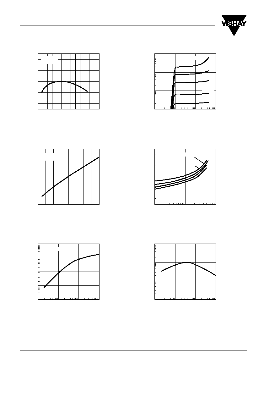
Figure 5. Relative Current Transfer Ratio vs. Ambient
Temperature
Figure 6. Collector Dark Current vs. Ambient Temperature
Figure 7. Collector Current vs. Forward Current
0.5
0.6
0.7
0.8
0.9
1.0
1.1
1.2
1.3
1.4
1.5
≠30≠20≠10 0 10 20 30 40 50 60 70 80 90 100
T
amb
≠ Ambient Temperature (∞C )
14391
CTR
≠
R
elative
Current
T
ransfer
Ratio
rel
V
CE
=5V
I
F
=1mA
1
10
100
1000
10000
100000
20
30
40
50
60
70
80
90
100
T
amb
≠ Ambient Temperature (∞C )
14392
I
≠
Collector
Dark
Current,
CEO
with
open
Base
(
n
A
)
V
CE
=10V
I
F
=0
0.1
1.0
10.0
100.0
1000.0
0.1
1.0
10.0
100.0
I
F
≠ Forward Current ( mA )
14393
V
CE
=2V
I
≠
Collector
Current
(
m
A
)
C
Figure 8. Collector Current vs. Collector Emitter Voltage
Figure 9. Collector Emitter Saturation Voltage vs. Collector Current
Figure 10. Current Transfer Ratio vs. Forward Current
0.1
1.0
10.0
100.0
0.1
1.0
10.0
100.0
V
CE
≠ Collector Emitter Voltage ( V )
14394
I
≠
Collector
Current
(
m
A
)
C
1mA
0.5mA
0.2mA
0.1mA
I
F
=2mA
0.6
0.7
0.8
0.9
1.0
1.1
1
10
100
I
C
≠ Collector Current ( mA )
14395
V
≠
Collector
Emitter
Saturation
V
oltage
(
V
)
CEsat
CTR=200%
25%
50%
100%
10
100
1000
10000
0.1
1.0
10.0
100.0
I
F
≠ Forward Current ( mA )
14396
V
CE
=2V
CTR
≠
Current
T
ransfer
Rati
o(%)
TCMD1000 / TCMD4000
Document Number 83513
Rev. 1.6, 26-Oct-04
Vishay Semiconductors
www.vishay.com
5
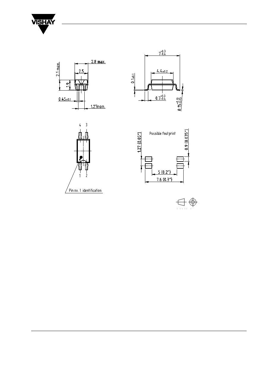
Package Dimensions in mm
16283